Here a brief overview of my research
Two main lines of research are currently ongoing:
Multi-scale simulations of nanoscale devices based on novel materials and architectures
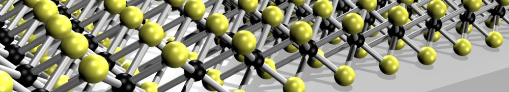
The aim is to investigate the potential of novel materials as  2D materials as graphene, Transition Metal Dichalcogenides or topological insulators able to comply with industry requirements in order to reach the goal of going More Moore and even Beyond CMOS, while suggesting new device concept, based on novel mechanisms (beyond the thermionic transport paradigm). Such a target can effectively be achieved through a multi-scale approach ranging from ab-initio calculations in order to get the mechanisms at play and extract the main physical parameters to feed transport simulations at the device level. Such approach represents, so far, the most powerful available tool in order to assess the real device potential and to provide guidelines to the fabrication side, as demonstrated by the articles available in the publication section.
Printable Electronics
The dream of obtaining printable electronic systems on any substrates either rigid or flexible as paper could be enabled by 2D materials as demonstrated by  the recent progress in the field. Conductive, insulating, or semiconducting inks can indeed be obtained through the exploitation of different 2D materials (e.g., graphene, hBN, or MoS2, respectively), which can also be combined in heterostructures, enlarging the degree of freedom and the device phase space. Our goal is to propose, fabricate and measure new inkjet printed device concepts through a synergic interaction between the simulation and the experimental activity recently started here in Pisa, and in tight collaboration with Manchester University (see publication section).
The goal is to define in the short/mid term all the main electronic building block (e.g. passive and active electronic components), in order to obtain a fully printable complete electronic system on flexible substrate as paper.